Transistor Manufacturing Techniques
Transistor Definition
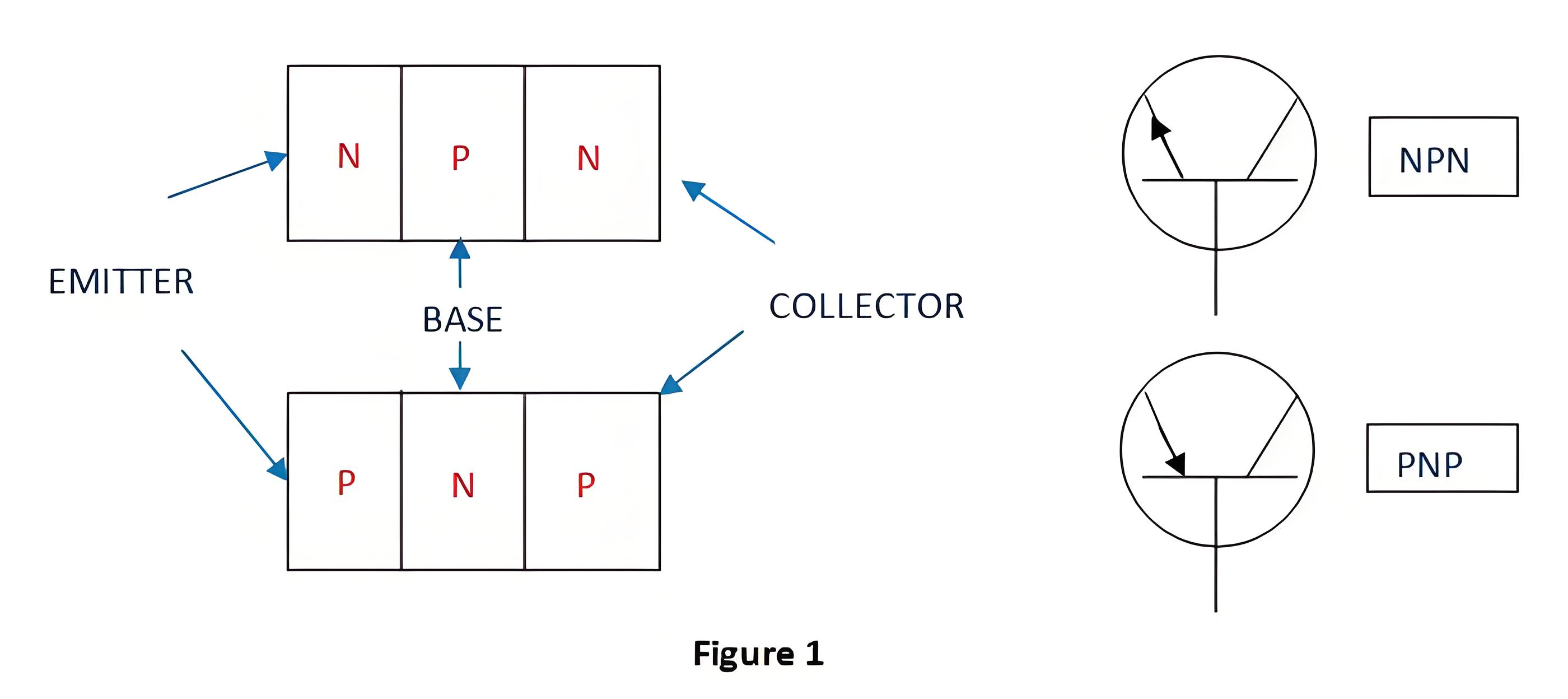
A transistor is a semiconductor device used to amplify or switch electronic signals and electrical power.
Diffused Technique
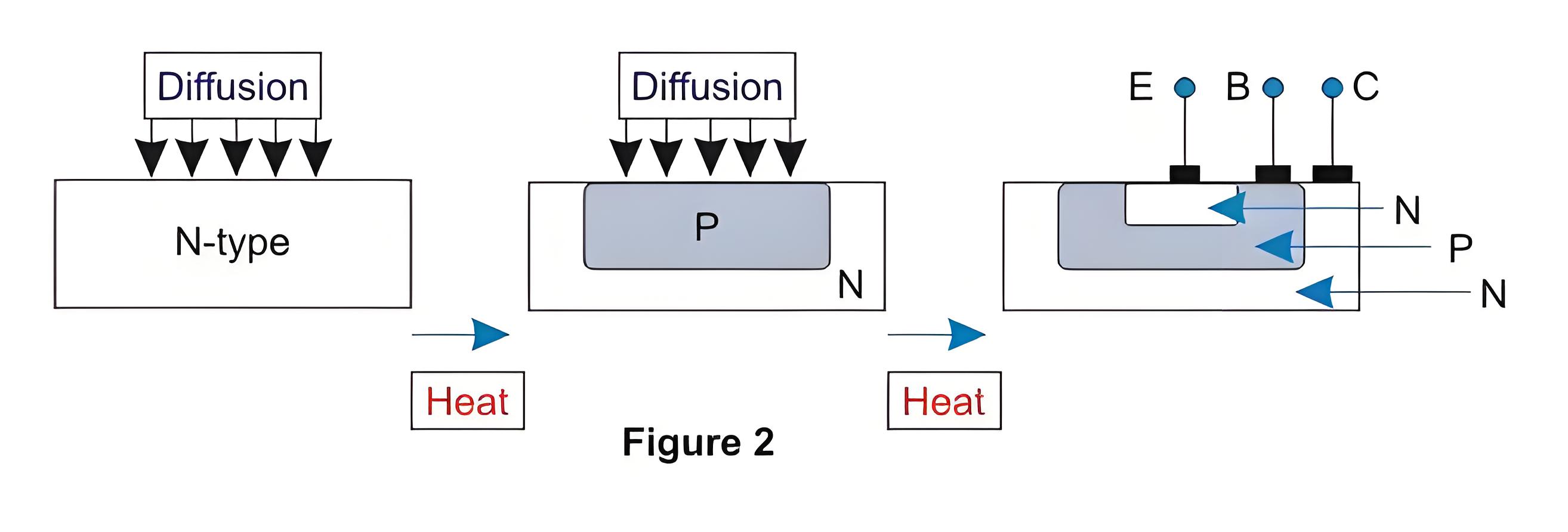
This method creates planar transistors on a nearly flat wafer. An N-type wafer is heated in a furnace with P-type gas impurities, causing the P-type region (base) to form on the wafer. A mask with holes is used, and the wafer is heated again with N-type impurities. This creates the N-type region (emitter) on top of the P-type layer.
At last, a thin layer of silicon dioxide is developed over the entire surface and photo stamped to create aluminium contacts for the leads of base and emitter.
Point Contact Technique
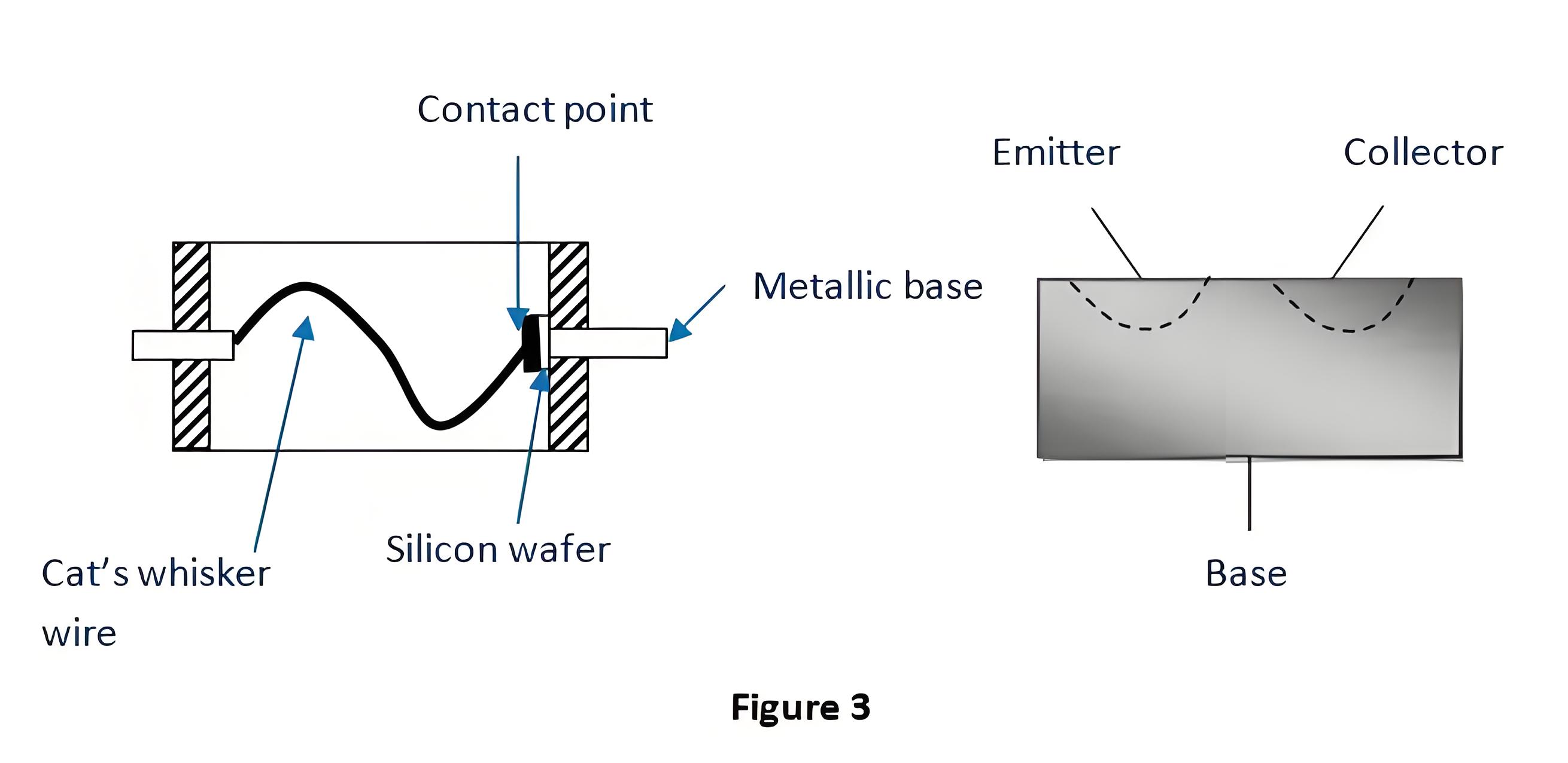
This technique uses an N-type semiconductor wafer, soldered to a metallic base. A tungsten spring (Cat’s whisker wire) is pressed against it, and the whole setup is enclosed in glass or ceramic for strength. A large current is passed briefly to create a PN junction at the contact point, making these transistors useful for high frequencies due to their low capacitance.
Fused or Alloy Technique
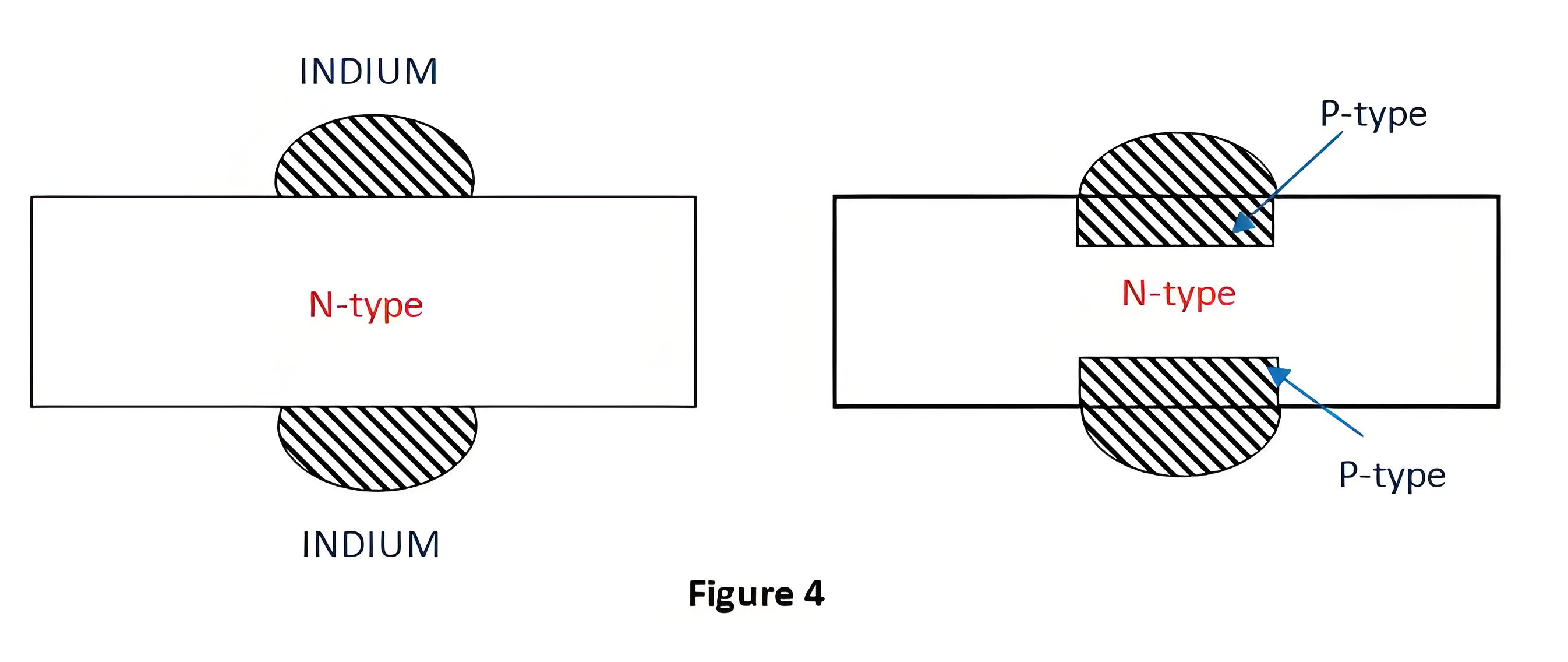
In this method, two tiny dots of indium or aluminium (acceptor) are positioned in the opposite side of n-type wafer. Then the whole system is heated to about a temperature which is less than the melting point of wafer material and greater than that of the acceptor.
A tiny portion of indium dissolves and enters into the wafer and thus the p-type material is created in the two sides of the wafer. The PNP transistor is created when it is cooled (figure 4).
Rate-Grown or Grown Technique
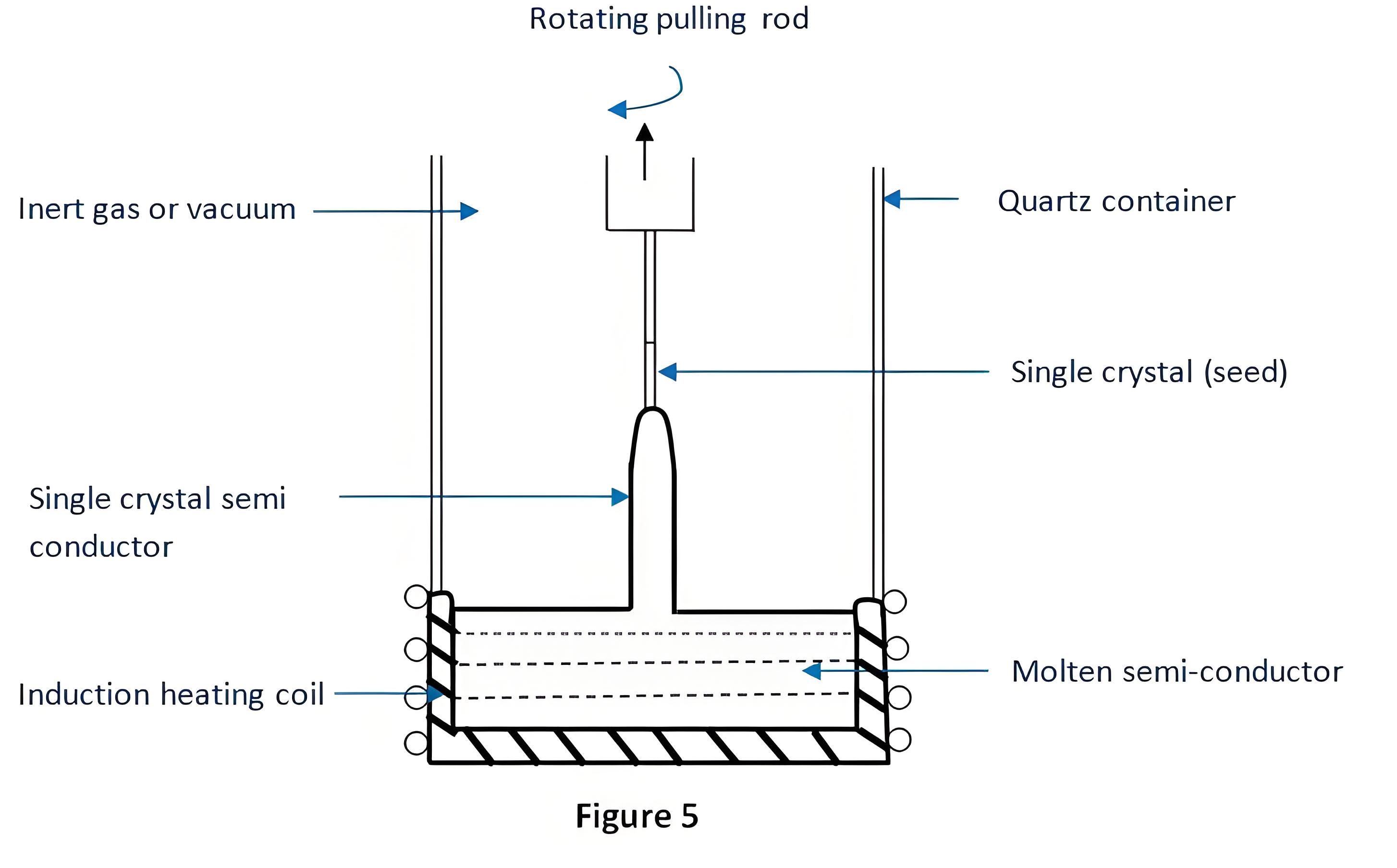
This method uses the Czochralski technique to draw a single crystal from a melt of Ge or Si with p-type impurities. A semiconductor seed is dipped into the molten semiconductor in a graphite crucible. The rod holding the seed is slowly rotated and withdrawn, first adding P-type impurities, then N-type, to grow a PN junction.
Epitaxial Technique
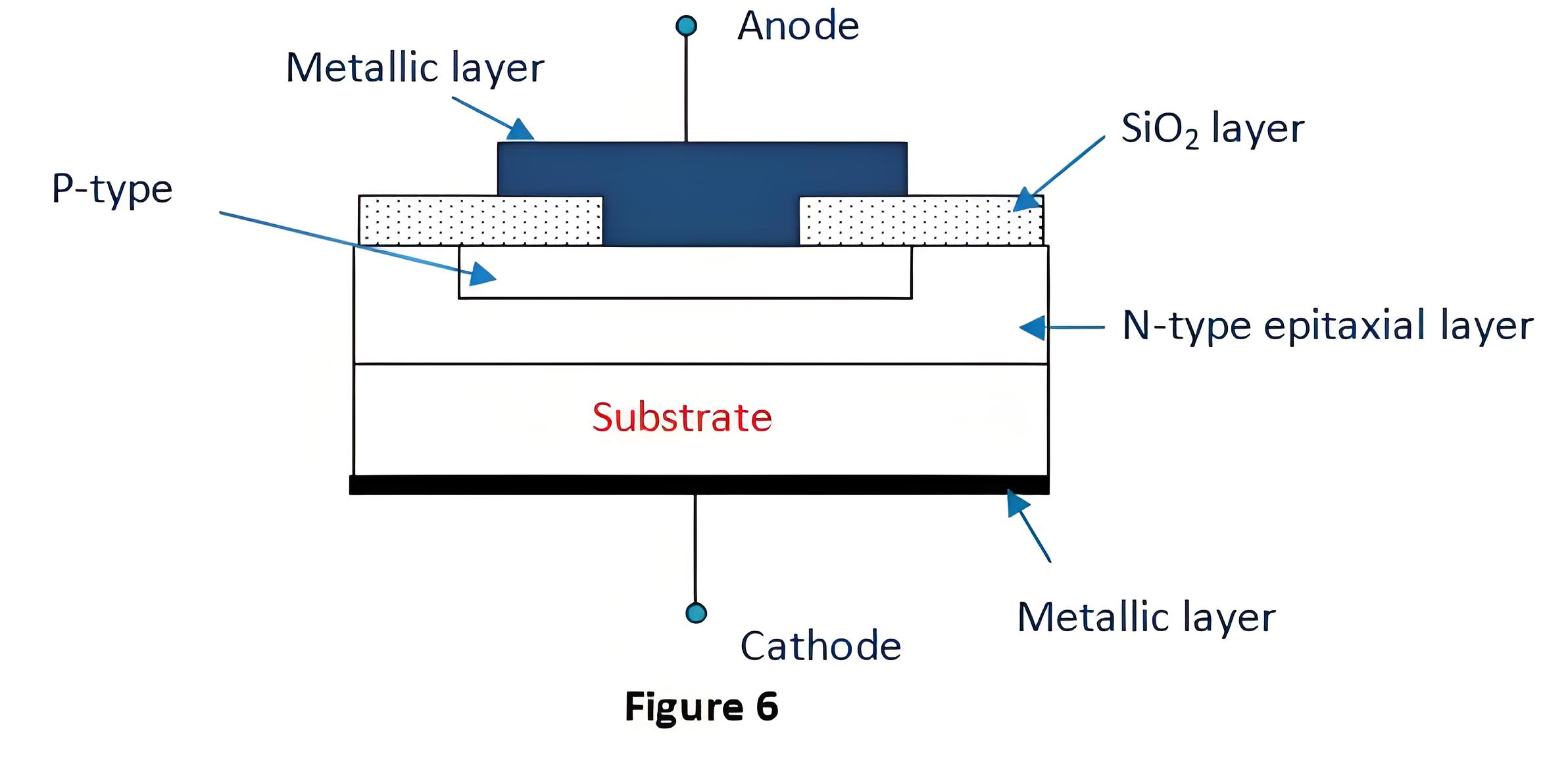
This method derives its name from Greek words meaning “on” and “arrangement.” A thin n-type Semiconductor or p-type semiconductor layer is grown on a heavily doped substrate of the same semiconductor. The formed layer can be the base, emitter, or collector, and the junction created has low resistance.
The Electricity Encyclopedia is dedicated to accelerating the dissemination and application of electricity knowledge and adding impetus to the development and innovation of the electricity industry.

